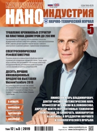
Femtoscan, 3d bioprinting, nanosurgery and biochips: threshold of scientific and technological breakthrough DOI: 10.22184/1993-8578.2019.12.5.240.245
The change in technological paradigms was marked by a transition to the nanotechnological level of substance research, including biological, the development of construction technologies at the biomacromolecular level, the creation of intelligent biochips and tools for nanosurgery and precision processing of materials within submicron accuracy. The scanning probe microscopy, together with related methods, has turned the study of the life secrets into an exciting research that lays the foundation for the upcoming scientific and technological breakthrough. Doctor of Physics and Mathematics, Professor of Lomonosov Moscow State University, Director of Advanced Technologies Center Igor Vladimirovich Yaminsky shares his thoughts, ideas and history of the digital nanoscopy development.
Titan dioxide nanopowder ceramics: SPS production method and properties Dense and solid fine-grained ceramics (microhardness of 16 GPA and grain size of 1µ) based on nanoscale titan dioxide powder was prepared by spark plasma sintering (SPS) method.
Differentiation of nanopowders on the size of particles on a transversely vibrating surface DOI: 10.22184/1993-8578.2019.12.5.250.255
The regularities of the acoustic method of separation of ultrafine powders — the redistribution of particles into nodes and the antinodes of a wave on the surface of a transversely oscillating plate — are considered. Experimental data on the efficiency of the separation of silica nanoparticles by this method were obtained. For the first time, the dependence of the characteristic size of the particle separation on the amplitude of oscillations smaller than the thickness of the Stokes boundary layer was revealed.
Reproducibility and stability of the technology and structural parameters of microelectronic devices DOI: 10.22184/1993-8578.2019.12.5.256.259
Considered are the technological approaches to ensure the achievement of a given
level of accuracy and stability of technological operations, the formation of instrument structures with specified parameters and devices on their basis.
Film thickness determination by spectroscopic reflectometry method using Fourier fast transform algorithms This paper presents examples of the software package intended to spectra treatment in order to determine thickness of films. Practical usage of TFCompanion (Semiconsoft) software as part of the MProbe® (Semiconsoft) measuring systems for reflected spectra’s analysis and thin films’ thickness calculation performed by embedded fast Fourier transform (FFT) algorithms is observed.
Deep anisotropic silicon etching with high aspect ratio for TSV structures Process of deep anisotropic silicon etching with alternating steps of etching and passivation process) is widely used for forming three-dimensional structures with through-silicon-vias, as well as in the manufacturing of micro electromechanical systems. The essence of the process lies in alternating steps of reactive-ion etching of silicon (usually SF6) and passivation of the surface (typically by using C4F8). Herewith the step of etching the passivation layer removing from the bottom of the grooves are faster than from the walls, with the result that allows to obtain anisotropic etching process. Advantages of the process include: carrying out the process at room temperatures, high photoresist selectivity (about 80:1 and more), the preparation of structures with an aspect ratio of 30:1, the etch rate up to 20 µm/min and controlled etching profile. The main drawback of the process is the roughness of the walls (scallops) in connection with the cyclical process. The aim of this work was to develop a reactor for deep silicon etching on wafers diameter of up to 200 mm, similar in their characteristics with import and development of technology deep silicon etching for its use in the manufacture of three-dimensional TSV assembly.
Machining center with automatic tool change Development of a small-size machining center having the abilities of an industrial milling machine presents a real alternative to the foreign products in the field of educational equipment. Such machining center enables to perform a great number of operations and the automatic change of tools after installing one blank without the intervention of an operator in order to improve accuracy of measurements, save time and serve as a visual aid in practical courses devoted to studying the equipment operation which reflects the maximum realistic conditions of manufacturing in full-size industrial solutions.
Methods of probe microscopy used for magnetic resonance tomography and spectroscopy Nowadays, the crucial task in the spectroscopy of biological objects in the natural media and magnetic resonance tomography is to increase the space and time resolution and sensitivity. It may be solved by combining the methods of scanning probe and NMR spectroscopy. It was shown that the original hardware and software platform permits to measure simultaneously the morphology, structure and molecular composition of biomacromolecules
immobilized on a hard substrate surface.
Ten best innovative products from "VacuumTechExpo 2019" Described are the best innovative products presented on the "VacuumTechExpo 2019" exhibition.
United scanning probe microscopy team United team of scientists is focused on developing of methods and equipment for bionanoscopy
and medical applications based on use of the scanning probe microscopy. One of the first researches dealing with biology was an investigation of differences in cell wall morphology of the initial and genetically modified bacteria.
Accelerators and business-incubators of Russian Federation in a field of nanotechnologies: from education startups to technological solutions World economics is on the verge of the new technological revolution because of nanotechnologies development. Today, nanotechnologies are the base of any technologies. In this paper we describe accelerators and business-incubators working in nanotechnologies on the basis of Russian institutes and universities. Presented are the just created examples of organized platforms and start-ups and already implemented technological solutions.

 rus
rus


